![[image of F3850 pin diagram]](images/f3850_pin.png)
![[image of F3851 pin diagram]](images/f3851_pin.png)
The 3859 and 3870 devices will also be covered on this page. Those units are actually single chip microcomputers and would be an alternative to the F8 rather than a supporting unit. All of the devices require a +5V and +12V source. With a 2MHz clock, instruction execution times range from 1 to 6.5 machine cycles or 2 to 13 microseconds.
Here is a pin diagram of the 3850 CPU and 3851 PSU.
The pin designation is as follows:
| Pin Name | Description | Data Flow |
|---|---|---|
| DB0 - DB7 | Data Bus Lines | Bidirectional |
| PHI, Write | Clock Lines | Output |
| I/O 00 - I/O 07 | I/O Port Zero | Bidirectional |
| I/O 10 - I/O 17 | I/O Port One | Bidirectional |
| ROMC0 - ROMC4 | Control Lines | Output |
| EXT RES | External Reset | Input |
| INT REQ | Interrupt Request | Input |
| ICB | Interrupt Control Bit | Output |
| RC | Clock Oscillator | Input |
| XTLX | Crystal Clock Line | Output |
| XTLY | External Clock Line | Input |
| Vss, Vdd, Vgg | Power Lines |
The 3850 CPU is consists of only the following:
The two main advantages of not having memory address logic on the CPU:
This diagram shows the organization of the F8 system registers.
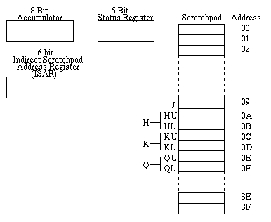
Note, there is one 8-bit Accumulator. The 64-byte scratchpad area can be thought of as 64 bytes of RAM, or as 64 8-bit secondary Accumulators. The instruction set allows the first 11 bytes to be accessed directly as secondary Accumulators. The other bytes can only be accessed using a type of implied addressing where the ISAR (Indirect Scratchpad Address Register) identifies the scratchpad RAM location. Since the 3850 does not have a Program Counter, Data Counter, or Stack Pointer, these registers are provided by the suport chips. The instruction set provides for register to register moves that move data between the scratchpad RAM and the Program Counter, Data Counter, or Stack Pointer. On the 3851 PSU, 3852 DMI, and the 3853 SMI devices, a 16-bit Data Counter (DC0), a 16-bit Data Counter Buffer (DC1), a 16-bit Program Counter (PC0), and a 16-bit Stack Pointer (PC1) are implemented.
Since address registers are present on every PSU, DMI or SMI device in an F8 system, these registers will be duplicated in any system that has more than a minimum amount of memory. As long as the sytem is correctly configured, this should present no problem.
 last modified 15MAR00
this home page is maintained by
Lowell O. Turner.
 Please email
lowell.turner@ieee.org with comments and corrections.
Please email
lowell.turner@ieee.org with comments and corrections.