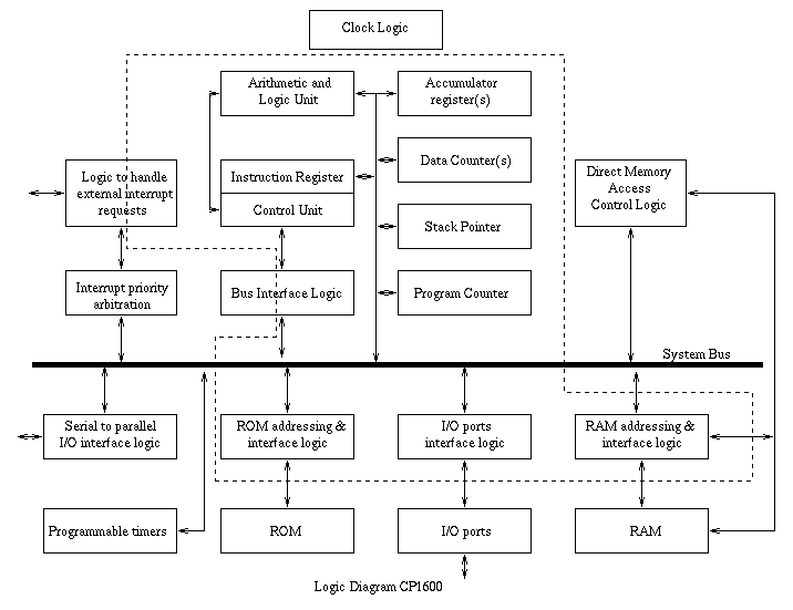
 The CP1600 logic diagram
The CP1600 is similar in structure to the single chip MicroNova covered elsewhere on this web page. It's instruction set as well it's execution speed is comparable to the National Semiconductor PACE also covered elsewhere on this web page. However, unlike the Pace, the CP1600's instruction set does not have any indirect addressing modes. This "feature" allows it to execute programs more than twice as fast as the PACE.
The CP1600 is heavily influenced by the DEC PDP-11. An important fact of the time is that the unit's signals are TTL compatible. However, buffers are still required to implement a complete system. It was constructed using NMOS ion implant technology. the unit comes in a 40 pin DIP and requires three (+12, +5, -3) power supplies. With a 200 nS (5 MHz) clock, instructions execute within 1.6 and 4.8 microseconds.
The CP1600 logic diagram
NOTE: The area inside the dotted line represents on chip units.
Note that it requires external logic to provide the timing required for operation. To implement an actual system, an address latch or buffer is needed since the data and address lines are multiplexed on a single 16-bit bus. As mentioned before, buffers to drive the components connected to the CPU. A one of eight decoder will also be necessary to produce the eight individual control signals out of the three coming from the device. Finally, a one of sixteen multiplexer to feed the 16 external status signals into the CPU.
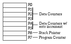 There are eight 16-bit registers.
Notice that all eight registers can be addressed as though they were general purpose registers. However, only register R0 has no other function assigned to it. Through this view, R0 can be thought of as the primary accumulator.
R1, R2, R3 can be used as data counters while R4 and R5 can be used as auto incrementing data counters. For example, instructions that make references to memory can use R4 or R5 to hold the implied address. Once the operation has completed, the register would be incremented. Registers R6 & R7 are the stack pointer and program counter. Obviously, if the executing program needs the stack, there will be two registers that cannot be used as "general purpose". As anyone who has had experience with the PDP-11 knows, (I was not one of those people) this is accessing the program counter directly allows for conditional branching and the ability to have multiple stacks is available when R6 is used for indexing purposes.
The CP1600 uses memory mapped I/O. That is, memory and I/O share a single address space. This allows the use of all addressing modes when operating on I/O.
Direct addressing instructions are two to three words (32 to 40 bits) where the second or last word provides a 16 bit direct address.
The instructions that reference memory via implied addressing use R1, R2, or R3 to hold the implied address. Note: when R4 or R5 is used, the contents will automatically be incremented following the instruction execution.
Since the CP1600 has no explicit stack manipulation instructions, (i.e. push, pull, or pop) the memory reference instructions that use R6 prvide for stack like behavior. For example, when R6 provides an implied address, it treated as an upward moving stack pointer. When a write operation uses implied addressing with R6, the register is incremented following the write operation. Similarly, a read operation using R6 as the implied address is decremented prior to the operation. Secondary memory refefence instructions using R6 have the effect of a "pop" or pull instruction. Logically, this register is a data counter with post increment and pre-decrement.
The CP1600 has four flags that would be recognized as "standard"
Four control signals are output allowing external logic to send an input in resonse. The control signals (EBCA0-EBCA3) output the low order four bits of the object code when executing the Branch On External (BEXT) instruction. External logic can then choose to input a high, which allows the BEXT to take the branch, or a logic low, which causes the next instruction in the sequence to be executed. This allows for up to 16 external conditions to be tested with the external logic replying appropriately.
This is a pin diagram of the device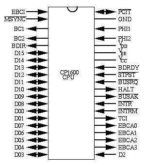
| Pin Name | Description | Pin Type |
|---|---|---|
| D00-D15 | Data and Address Bus | Bidirectional & Tristate |
| BDIR, BC1, BC2 | Bus Control Signals | Output |
| PHI1, PHI2 | Clock Signals | Input |
| MSYNC | Master Synchronization | Input |
| EBCA0-EBCA3 | External Branch Condition address lines | Output |
| EBCI | External Branch Condition input | Input |
| PCIT | Program Counter Inhibit/Software Interrupt Signal | Input |
| BDRDY | Wait signal | Input |
| STPST | CPU Stop/Start on negative edge transition | Input |
| HALT | Halt State signal | Output |
| INTR, INTRM | Interrupt Request Lines | Input |
| TCI | Terminate Current Interrupt | Output |
| BUSRQ | Bus Request | Input |
| BUSAK | External Bus Control Acknowledge | Output |
| Vbb, Vcc, Vdd, GND | Power Supply |
Because the bus is multiplexed, the signals BDIR, BC1, and BC2 are needed to identify the traffic on the bus at any time. As shown below and mentioned above, a one of eight decoder is needed to decode the three signals into the eight signals shown in the table below.
| BC1 | BC2 | BDIR | Signal Name | Function Description |
|---|---|---|---|---|
| 0 | 0 | 0 | NACT | The CPU is inactive and D00-D15 is in High Impedance state |
| 0 | 0 | 1 | BAR | A memory address must be input to the CPU via D00-D15 |
| 0 | 1 | 0 | IAB | A previously acknowledged interrupt must place the service routine's starting address on the bus. |
| 0 | 1 | 1 | DWS | Data write strobe for external memory. |
| 1 | 0 | 0 | ADAR | The bus is currently floating. This happens when the contents of a data counter register's contents are being used to compute the effective address during an implied addressing operation. |
| 1 | 0 | 1 | DW | The CPU is writing data to external memory. This signal will precede DWS by one machine cycle. |
| 1 | 1 | 0 | DTB | This is a read strobe which external devices can use when placing data on the D00-D15 bus. |
| 1 | 1 | 1 | INTAK | This is the interrupt acknowledge signal. IAB follows alerting the interrupting device to place the starting address of it's interrupt service routine on the D00-D15 bus. |
The other controls fall in the following major groups:
The Interrupt and DMA are covered in the next section. PHI1 and PHI2 are the system's clock inputs. They are complimentary (180 degrees out of phase) though the duty cycle need not be 50%.
The other timing signal is the MSYNC input. Following the system power up, this signal must be held low for at least ten milliseconds. After this, on the rising edge of MSYNC, CPU internal logic will synchronize the PHI1 and PHI2 clocks to start a new machine cycle. This is unusual in that most processors of the time had internal logic that handled this synchronization.
The other aspect of note involving this signal is that when the system is reset, no registers are modified not even the Program Counter! On the positive edge of MSYNC, the CPU reads D00-D15 and uses this value to point to the location of the instruction to be executed. This means that external logic must also receive this signal in order to put a valid address on the bus for the CPU to retreive.
Sorry, This section is incomplete
The instruction set is relatively standard. I have included the instruction set summary, as well as the op codes A table of the branch conditions and corresponding codes is also at that link.
The CP1600 Electrical Data (That I have access to) is available here.
 last modified 10JUL01
this home page is maintained by Lowell O. Turner.
 Please email
lowell.turner@ieee.org with comments and corrections.
Please email
lowell.turner@ieee.org with comments and corrections.